Gravitacija Polprevodniki
Raziskave na področju polprevodniških materialov in polprevodniških naprav


Predstavitev
Cilji projekta in kratek povzetek vsebine projekta

Raziskovalna področja
Pregled raziskovalnih področij, ki jih člani konzorcija pokrivajo

Člani konzorcija
Predstavitev raziskovalnih inštitucij, ki sodelujejo v projektu
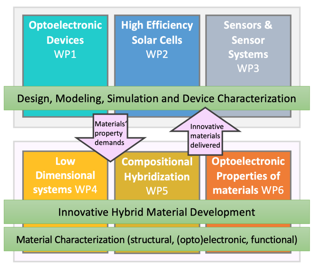
Device-oriented Research

Optoelectronic devices
Development of improved solutions of dedicated integrated photonic components and circuits, photonic chip-to-fiber coupling solutions, power-over-fiber & on-chip-power and improved perovskite led emitting diodes.

High Efficiency Solar Cells
Development of highly efficient perovskite/perovskite tandem solar cells for outdoor and indoor operation, and recombination layer to connect the two subcells.

Sensors & Sensor Systems
Design and demonstration of photonic-SC sensors and sensors systems. The focus is on the development of new sensors and sensor systems based on either fiber optic structures or PICs, or a combination of both.
Materials-oriented Research

Low Dimensional systems
Synthesis/preparation of novel semiconducting one- and two-dimensional materials and their heterostructures. Feasibility studies of optoelectronic (OE) properties. Optimization of OE effects
for improved performance in photonic applications. Study of Pockels, Kerr
and quantum-confined Stark effects, interfaces between different
materials components, and between silicon-based materials and novel low-dimensional systems.

Compositional Hybridization
Design and synthesis of composite and hybrid materials from low dimensional systems, i.e., QDs and 2DMs, for improved performance in photonic applications including voltage/electric field
sensors, biomedical sensor, photovoltaic and photonic devices.

Optoelectronic Properties of materials
Fundamental studies of the effects of compositional hybridization on the optoelectronic (OE) properties. Extensive
characterisation of novel OE materials, using time-resolved UPS, XPS, and computational physics-based modelling. First-principles modelling of the size-related effects,
interface interactions, and doping.
Collaborative research to novel semiconductors and devices
The project is organized in two levels, combining the expertise of the participating research organization.
The DEVICE level covers device aspects from design, modelling and simulations to fabrication and
characterization. The MATERIALS level supports the Device level development through innovative hybrid
materials development, promoting new materials solutions and fundamental knowledge on their properties.

Contact
address:
Projekt Gravitacija
Vipavska 11c
SI-5270 Ajdovščina
Slovenija

